P - Pmna
1. Structure Summary
Last Updated |
2022-12-09 |
Crystal Prototype |
A |
Crystal System |
Rectangular |
Lattice Constant a (Å) |
3.304 |
Lattice Constant b (Å) |
4.616 |
Space Group |
Pmna |
Formation Energy (eV/f.u.) |
0.0785 |
2. Mechanical Properties (PBE)
2.1 Stiffness Tensors
Cij (N/m) |
xx |
yy |
zz |
xx |
104.479 |
21.585 |
0.000 |
yy |
21.585 |
34.019 |
0.000 |
zz |
0.000 |
0.000 |
27.402 |
2.2 Compliance Tensors
Sij (m/N) |
xx |
yy |
zz |
xx |
0.011015 |
-0.006989 |
0.000000 |
yy |
-0.006989 |
0.033830 |
0.000000 |
zz |
0.000000 |
0.000000 |
0.036494 |
2.3 Orientation-Dependent Mechanical Properties
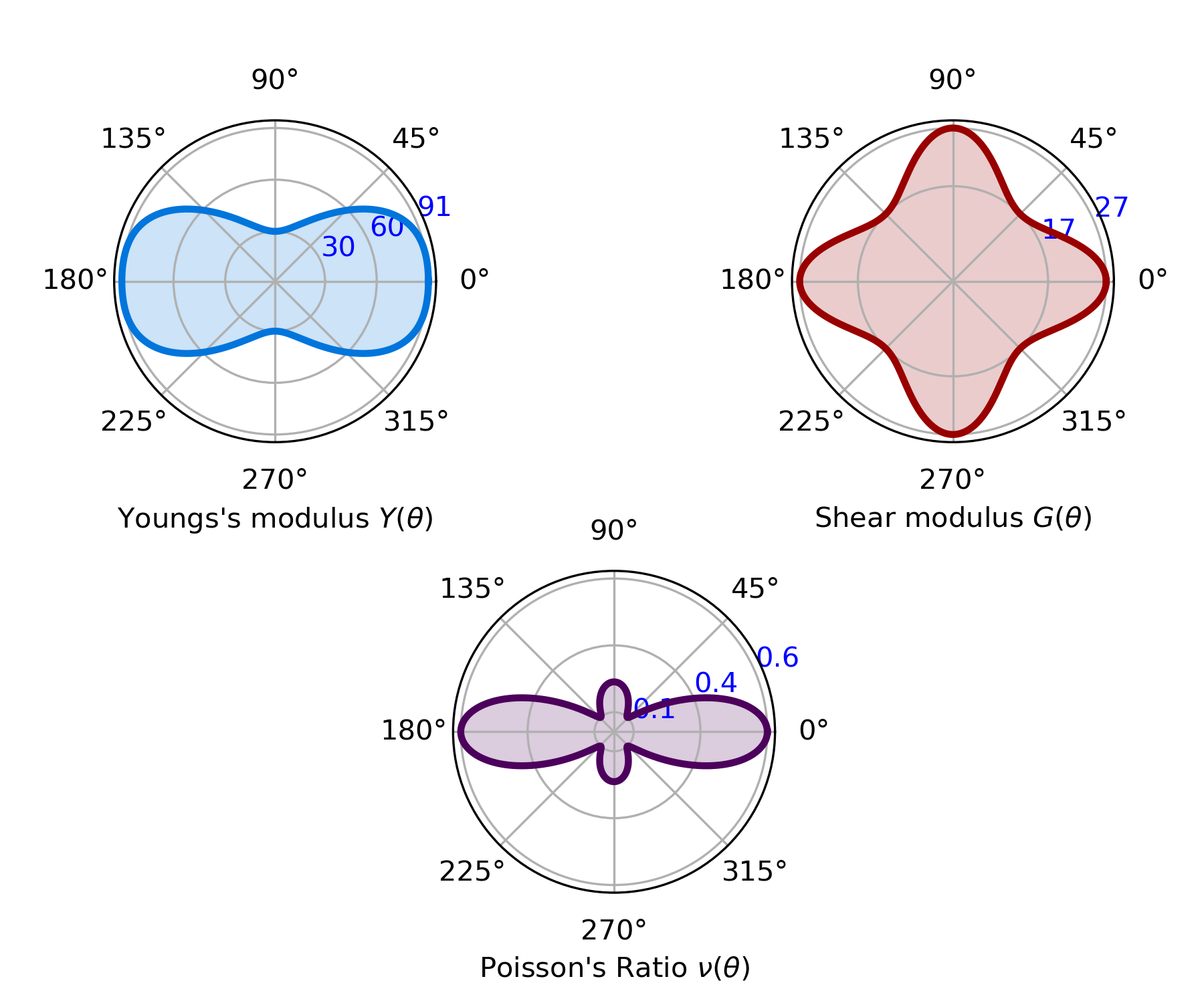
2.4 Anisotropic Mechanical Properties Of 2D Singlecrystal
Mechanical Properties |
Min |
Max |
Anisotropy |
Young’s Modulus (N/m) |
29.560 |
90.783 |
3.071 |
Shear Modulus (N/m) |
17.000 |
27.402 |
1.612 |
Poisson’s Ratio |
0.081 |
0.634 |
7.827 |
2.5 Anisotropic Mechanical Properties Of 2D Polycrystal
Mechanical Properties |
Min |
Max |
Anisotropy |
Young’s Modulus (N/m) |
45.417 |
32.397 |
3.071 |
Shear Modulus (N/m) |
25.617 |
20.983 |
1.612 |
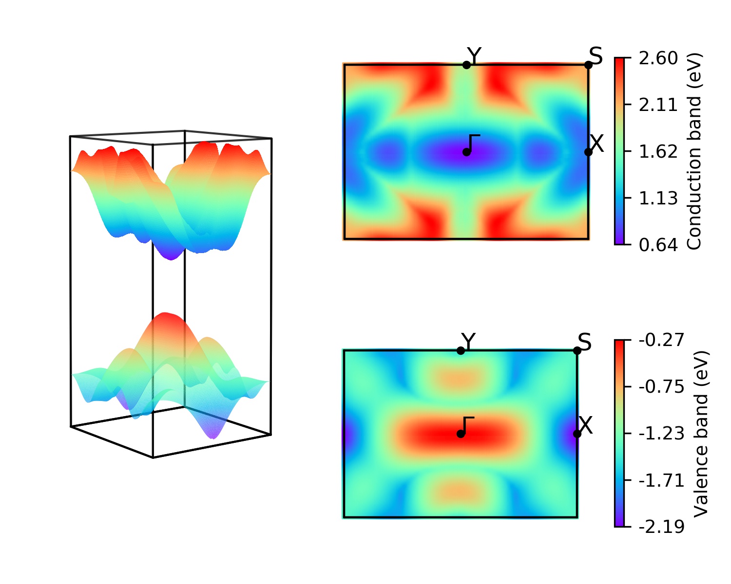
3. Fundmental Electronic Properties
Band Character |
Direct |
Band Gap (PBE, eV) |
0.9161 |
Band Gap (HSE, eV) |
1.6093 |
Ionization Energy (HSE, eV) |
-5.461 |
Electron Affinity (HSE, eV) |
-3.892 |
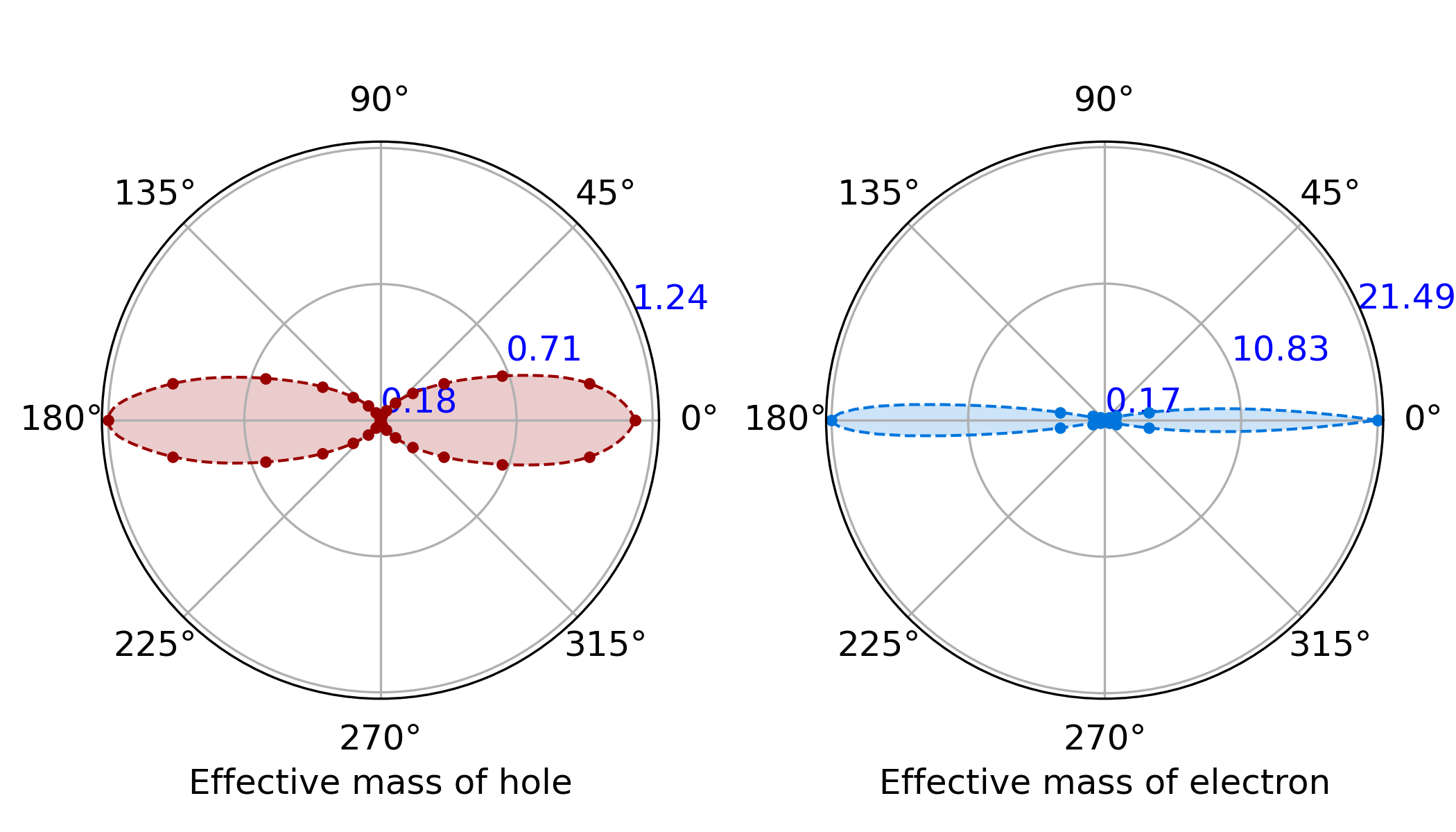
Effective Mass of Electron Max. (m0) |
1.244 |
Effective Mass of Electron Min. (m0) |
0.183 |
Effective Mass of Hole Max. (m0) |
21.489 |
Effective Mass of Hole Min. (m0) |
0.167 |
Location of Valence Band Maximum |
[0.000000, 0.000000] |
Location of Conduction Band Minimum |
[0.000000, 0.000000] |
3.1 Global Band Structure (PBE)
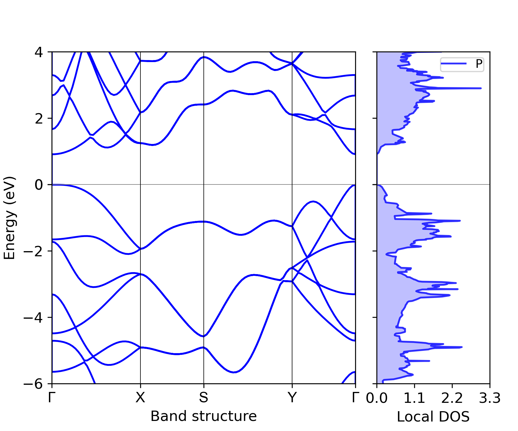
3.2 Band Structure and Density of States (PBE)
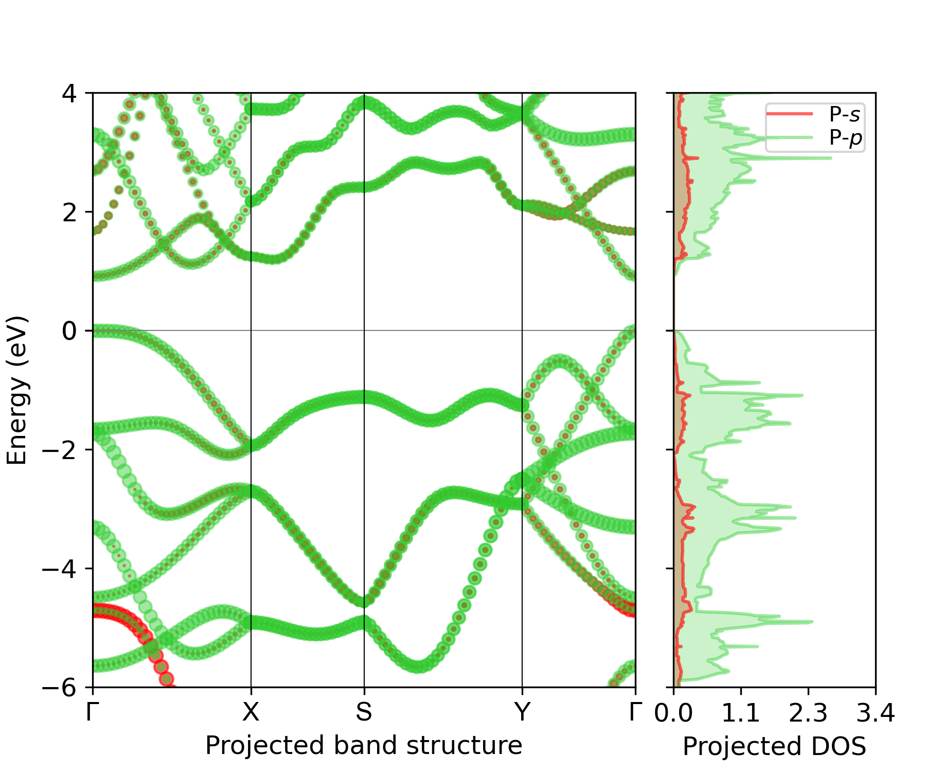
3.3 Projected Band Structure and Density of States (PBE)
3.4 Orientation-Dependent effective Masses (PBE)
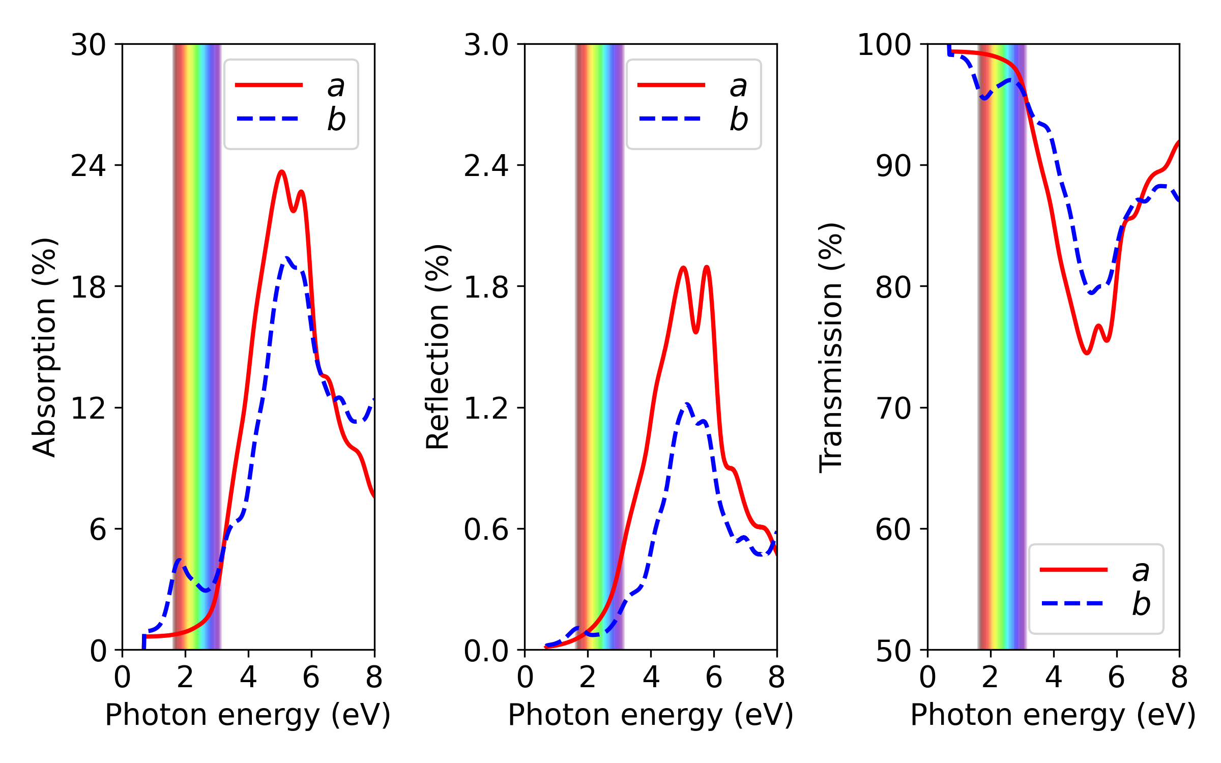
4. Optical Spectrums (HSE)
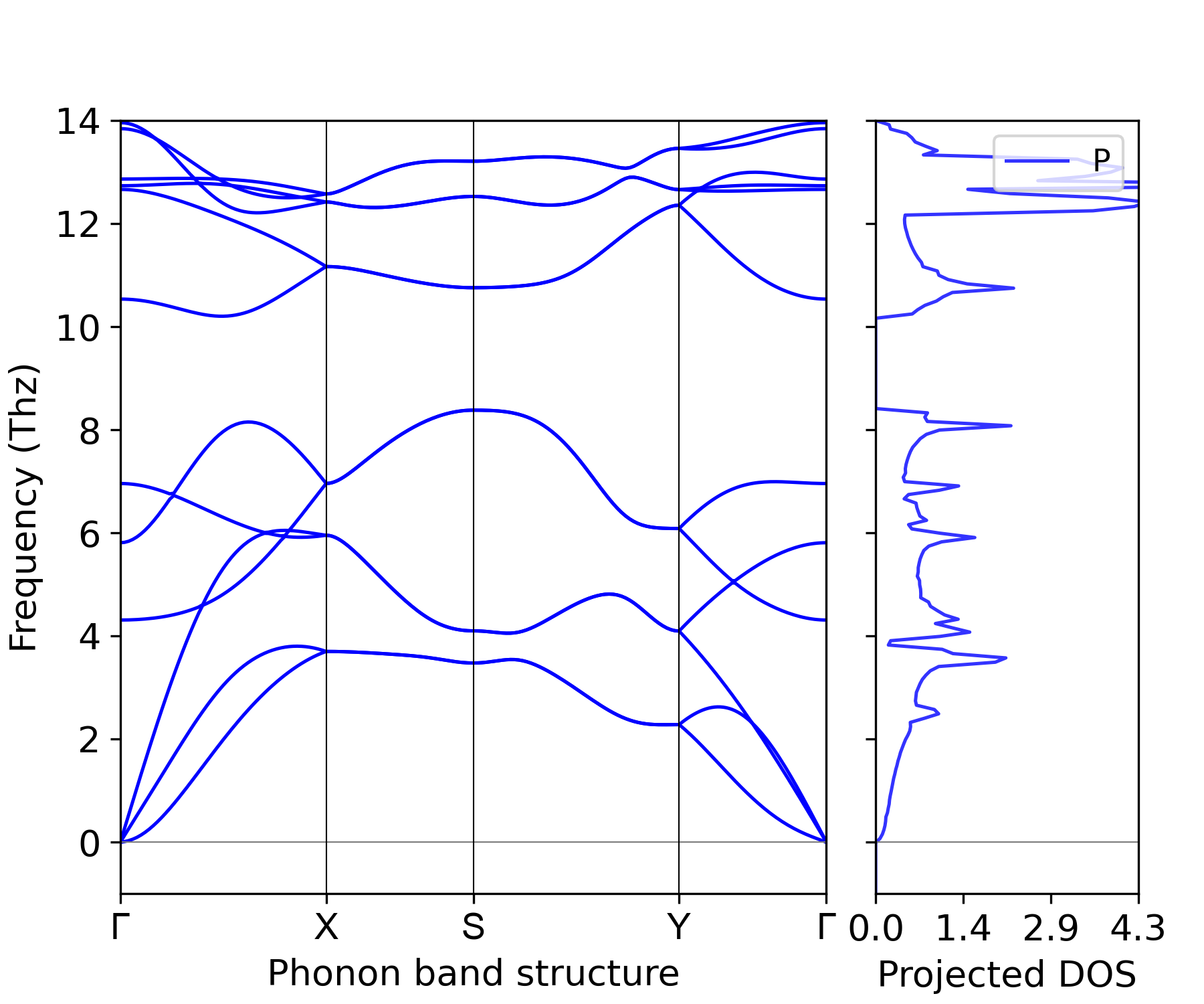
5. Phonon Spectrum and Density of States (PBE)
References
Note
For more details of this database, please refer to the following reference.
[1] V. Wang, G. Tang, Y.-C. Liu, R.-T. Wang, H. Mizuseki, Y. Kawazeo, J. Nara, W.-T. Geng, High-Throughput Computational Screening of Two-Dimensional Semiconductors, Journal of Physical Chemistry Letters 13, 11581 (2022).
License
The contents of this web page are licensed under a Creative Commons 4.0 Attribution International License unless another license is specially mentioned in each web page.