PbS - Aem2
1. Structure Summary
Last Updated |
2022-12-09 |
Crystal Prototype |
AB |
Crystal System |
Square |
Lattice Constant a (Å) |
5.945 |
Lattice Constant b (Å) |
5.946 |
Space Group |
Aem2 |
Formation Energy (eV/f.u.) |
-0.8428 |
2. Mechanical Properties (PBE)
2.1 Stiffness Tensors
Cij (N/m) |
xx |
yy |
zz |
xx |
76.860 |
3.555 |
0.000 |
yy |
3.555 |
76.860 |
0.000 |
zz |
0.000 |
0.000 |
12.758 |
2.2 Compliance Tensors
Sij (m/N) |
xx |
yy |
zz |
xx |
0.013039 |
-0.000603 |
0.000000 |
yy |
-0.000603 |
0.013039 |
0.000000 |
zz |
0.000000 |
0.000000 |
0.078382 |
2.3 Orientation-Dependent Mechanical Properties
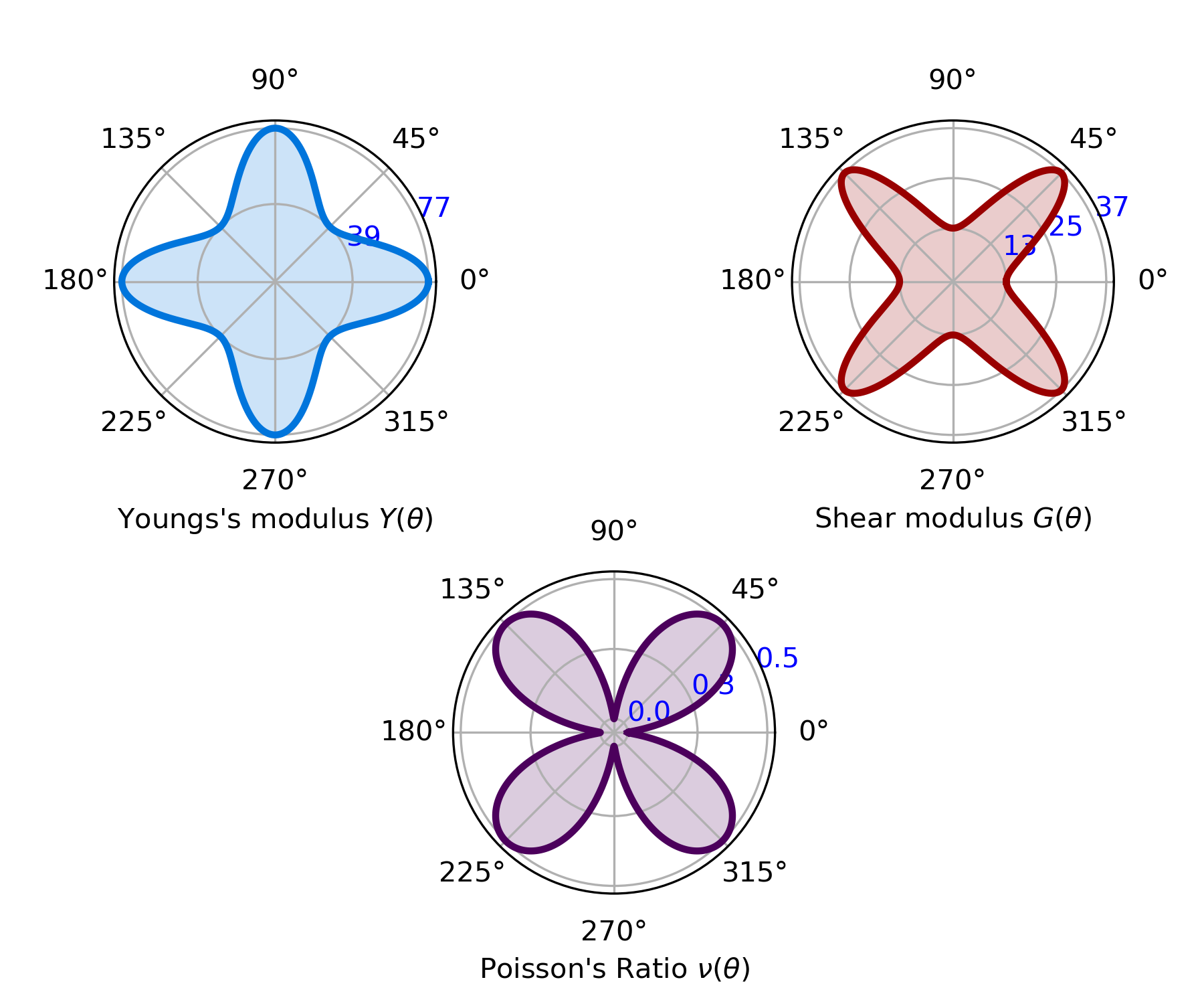
2.4 Anisotropic Mechanical Properties Of 2D Singlecrystal
Mechanical Properties |
Min |
Max |
Anisotropy |
Young’s Modulus (N/m) |
38.740 |
76.696 |
1.980 |
Shear Modulus (N/m) |
12.758 |
36.652 |
2.873 |
Poisson’s Ratio |
0.046 |
0.518 |
11.205 |
2.5 Anisotropic Mechanical Properties Of 2D Polycrystal
Mechanical Properties |
Min |
Max |
Anisotropy |
Young’s Modulus (N/m) |
40.208 |
40.207 |
1.980 |
Shear Modulus (N/m) |
24.705 |
18.928 |
2.873 |
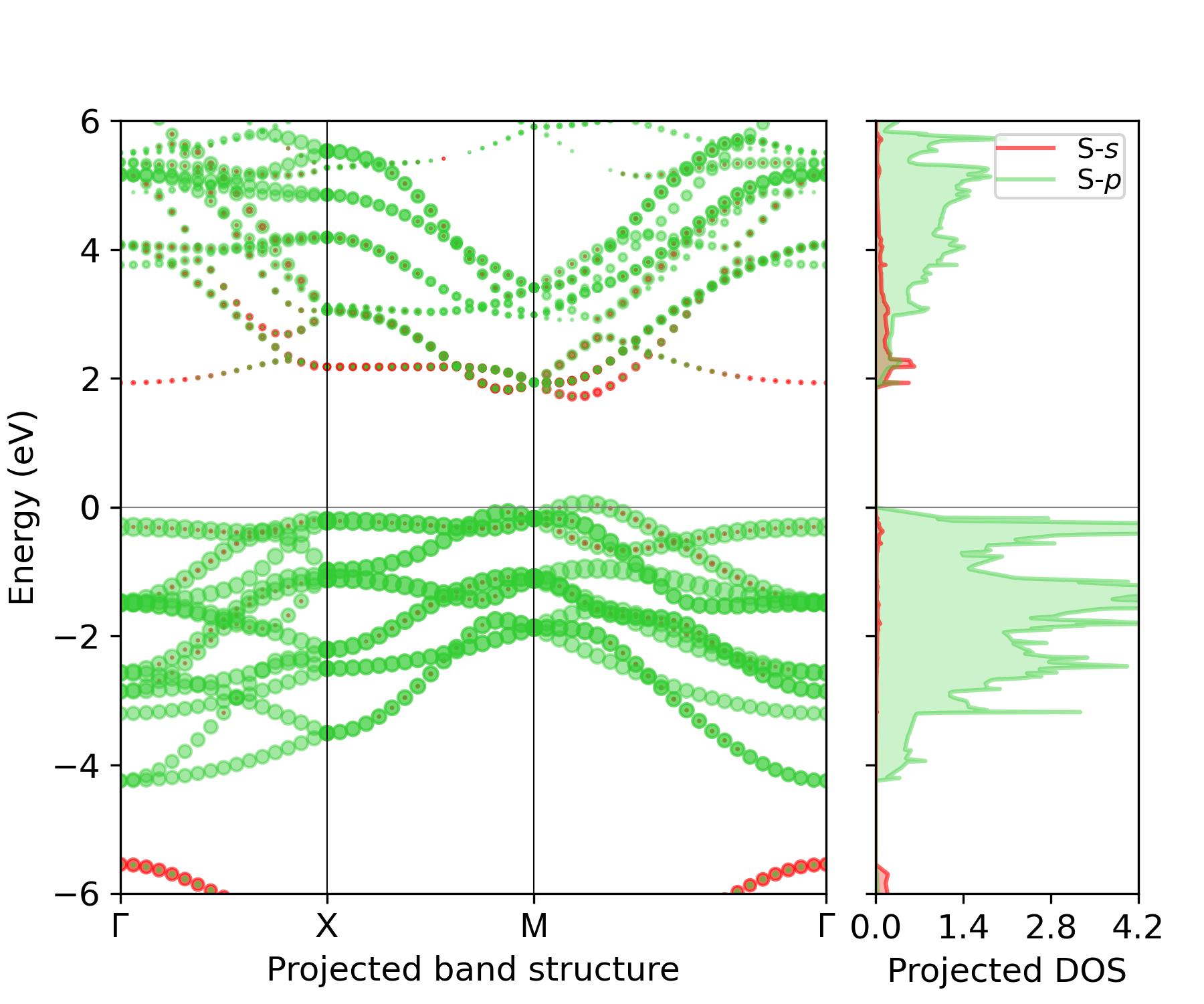
3. Fundmental Electronic Properties
Band Character |
Direct |
Band Gap (PBE, eV) |
1.6651 |
Band Gap (HSE, eV) |
2.2869 |
Ionization Energy (HSE, eV) |
-4.868 |
Electron Affinity (HSE, eV) |
-2.581 |
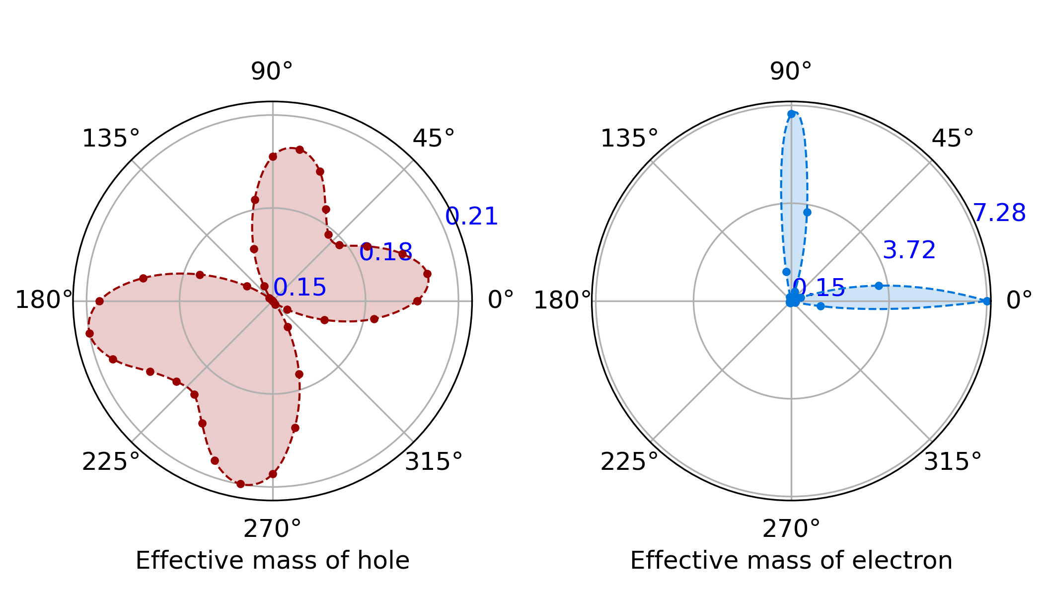
Effective Mass of Electron Max. (m0) |
0.213 |
Effective Mass of Electron Min. (m0) |
0.155 |
Effective Mass of Hole Max. (m0) |
7.280 |
Effective Mass of Hole Min. (m0) |
0.153 |
Location of Valence Band Maximum |
[0.409091, 0.409091] |
Location of Conduction Band Minimum |
[0.409091, 0.409091] |
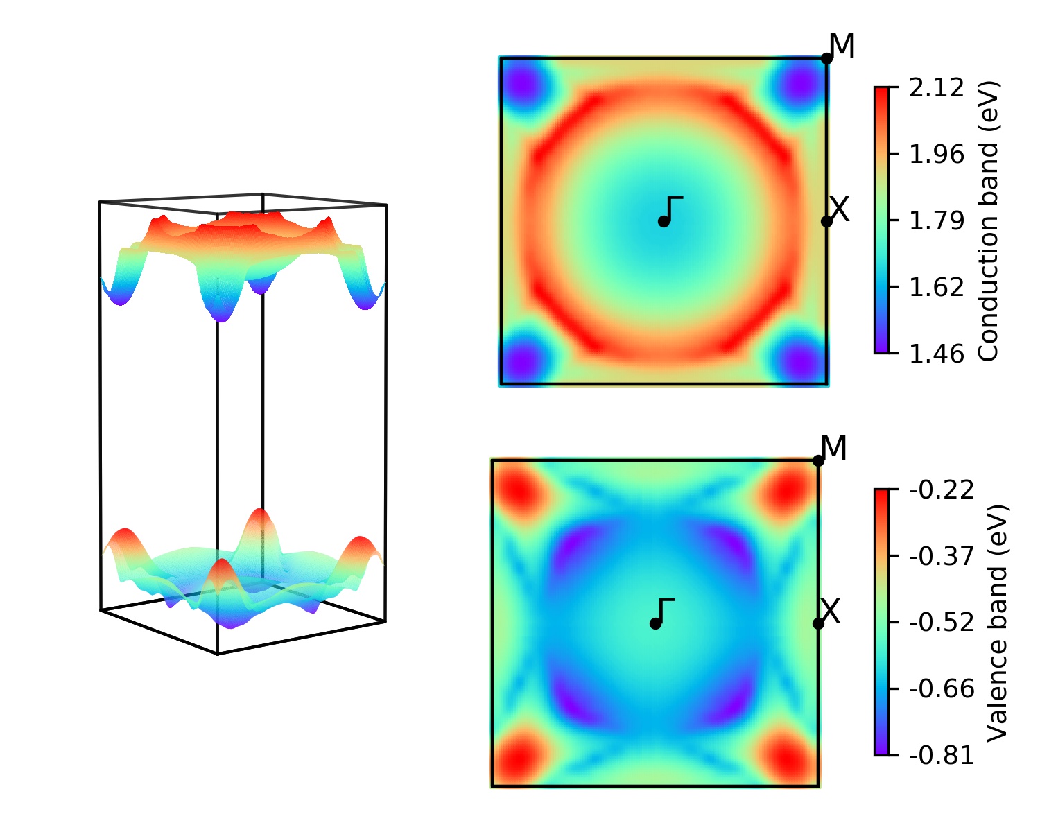
3.1 Global Band Structure (PBE)
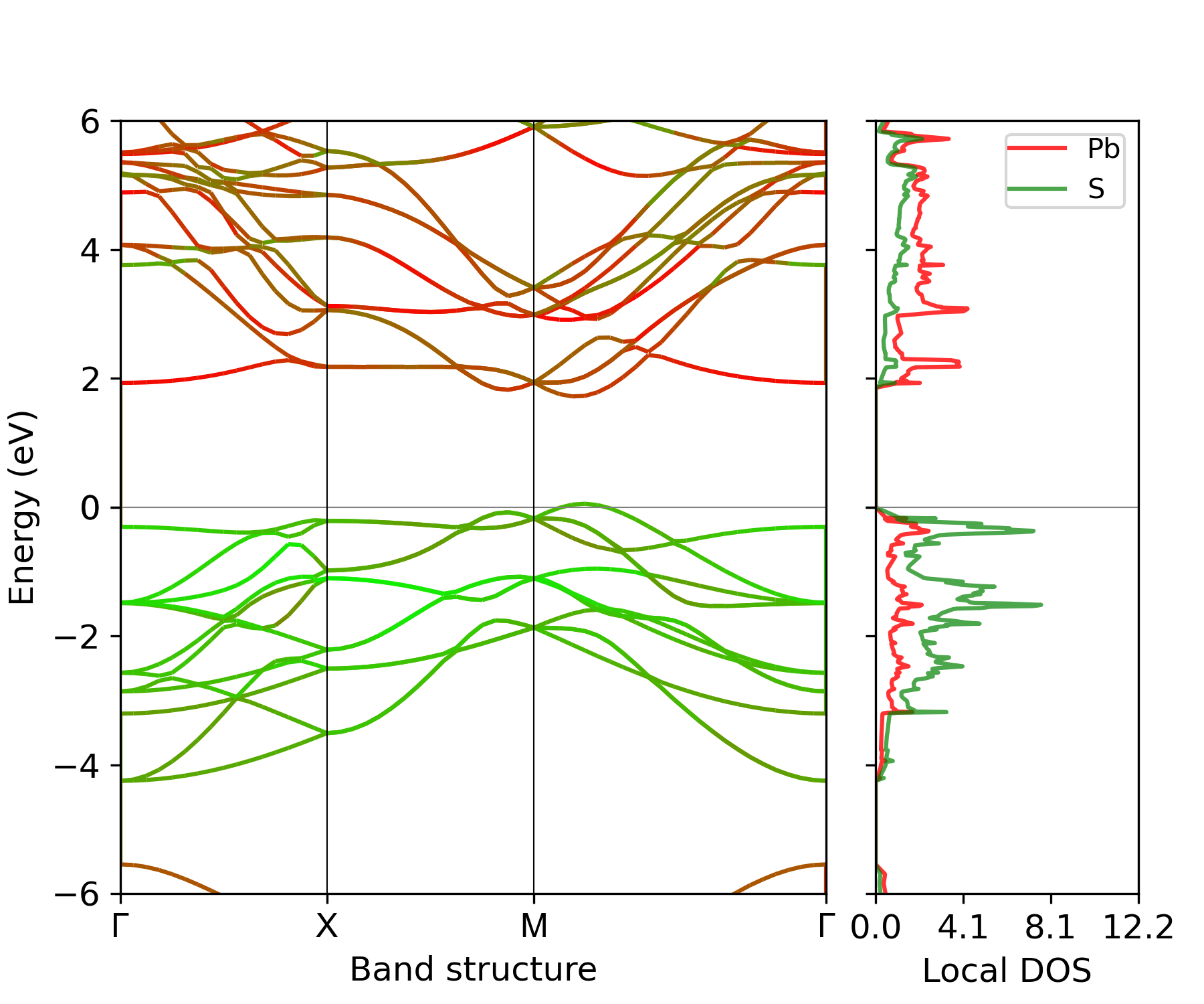
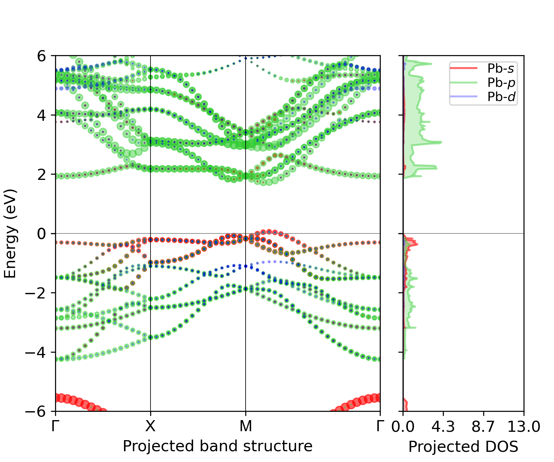
3.2 Band Structure and Density of States (PBE)
3.4 Orientation-Dependent effective Masses (PBE)
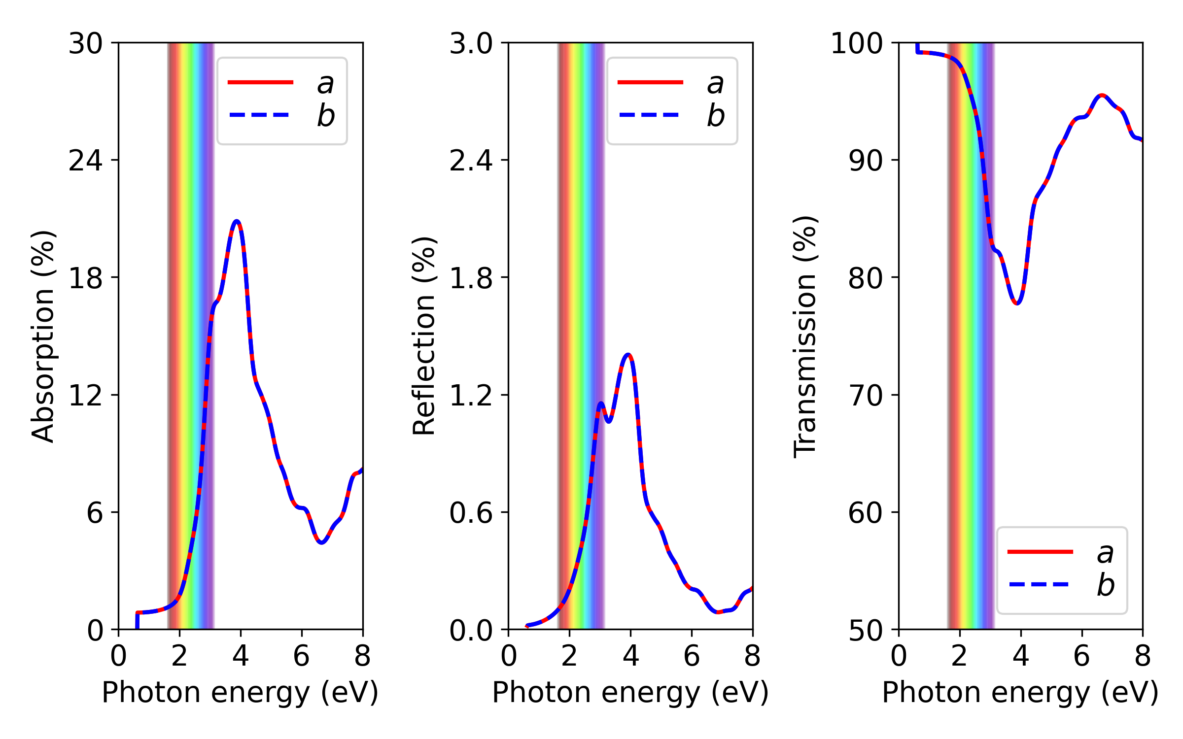
4. Optical Spectrums (HSE)
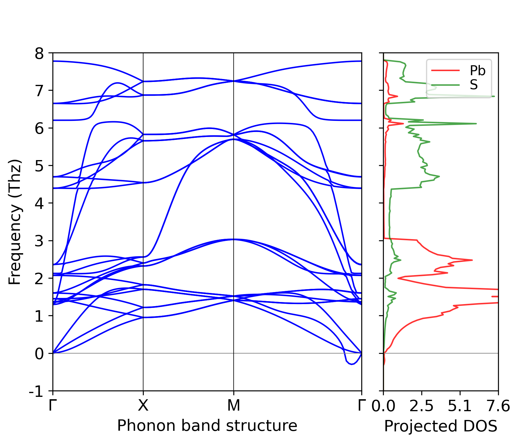
5. Phonon Spectrum and Density of States (PBE)
References
Note
For more details of this database, please refer to the following reference.
[1] V. Wang, G. Tang, Y.-C. Liu, R.-T. Wang, H. Mizuseki, Y. Kawazeo, J. Nara, W.-T. Geng, High-Throughput Computational Screening of Two-Dimensional Semiconductors, Journal of Physical Chemistry Letters 13, 11581 (2022).
License
The contents of this web page are licensed under a Creative Commons 4.0 Attribution International License unless another license is specially mentioned in each web page.