SiAs2 - Pmc2
1. Structure Summary
Last Updated |
2022-12-09 |
Crystal Prototype |
AB2 |
Crystal System |
Rectangular |
Lattice Constant a (Å) |
3.663 |
Lattice Constant b (Å) |
10.311 |
Space Group |
Pmc2 |
Formation Energy (eV/f.u.) |
0.0402 |
2. Mechanical Properties (PBE)
2.1 Stiffness Tensors
Cij (N/m) |
xx |
yy |
zz |
xx |
109.444 |
-0.082 |
0.000 |
yy |
-0.082 |
1.034 |
0.000 |
zz |
0.000 |
0.000 |
0.365 |
2.2 Compliance Tensors
Sij (m/N) |
xx |
yy |
zz |
xx |
0.009138 |
0.000725 |
0.000000 |
yy |
0.000725 |
0.967175 |
0.000000 |
zz |
0.000000 |
0.000000 |
2.739726 |
2.3 Orientation-Dependent Mechanical Properties
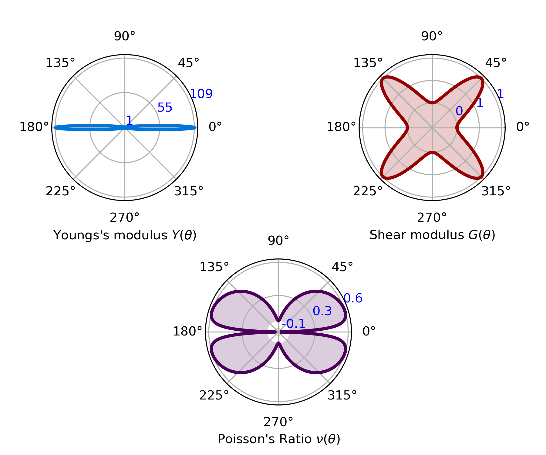
2.4 Anisotropic Mechanical Properties Of 2D Singlecrystal
Mechanical Properties |
Min |
Max |
Anisotropy |
Young’s Modulus (N/m) |
0.944 |
109.437 |
115.937 |
Shear Modulus (N/m) |
0.365 |
1.026 |
2.810 |
Poisson’s Ratio |
-0.079 |
0.600 |
-7.560 |
2.5 Anisotropic Mechanical Properties Of 2D Polycrystal
Mechanical Properties |
Min |
Max |
Anisotropy |
Young’s Modulus (N/m) |
27.579 |
1.023 |
115.937 |
Shear Modulus (N/m) |
14.013 |
0.538 |
2.810 |
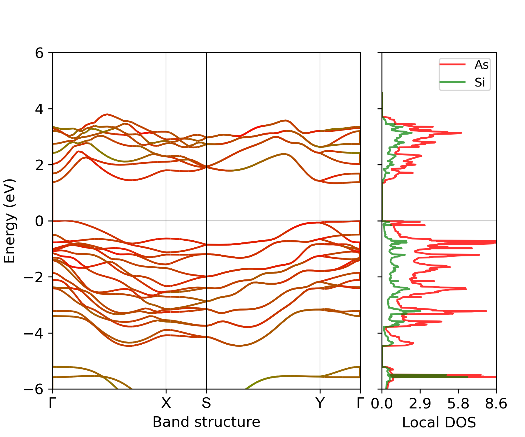
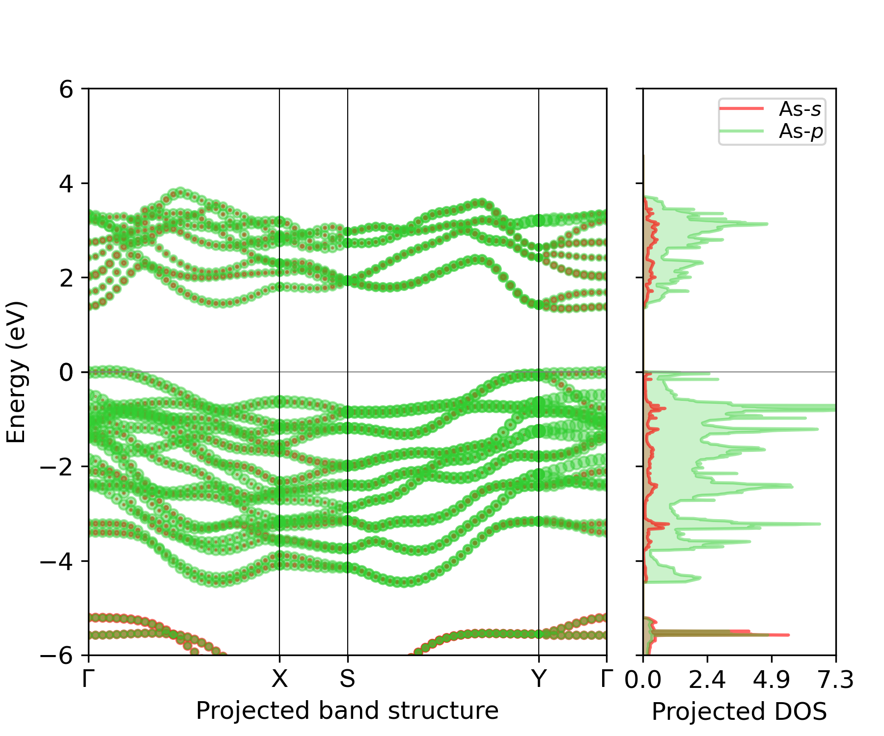
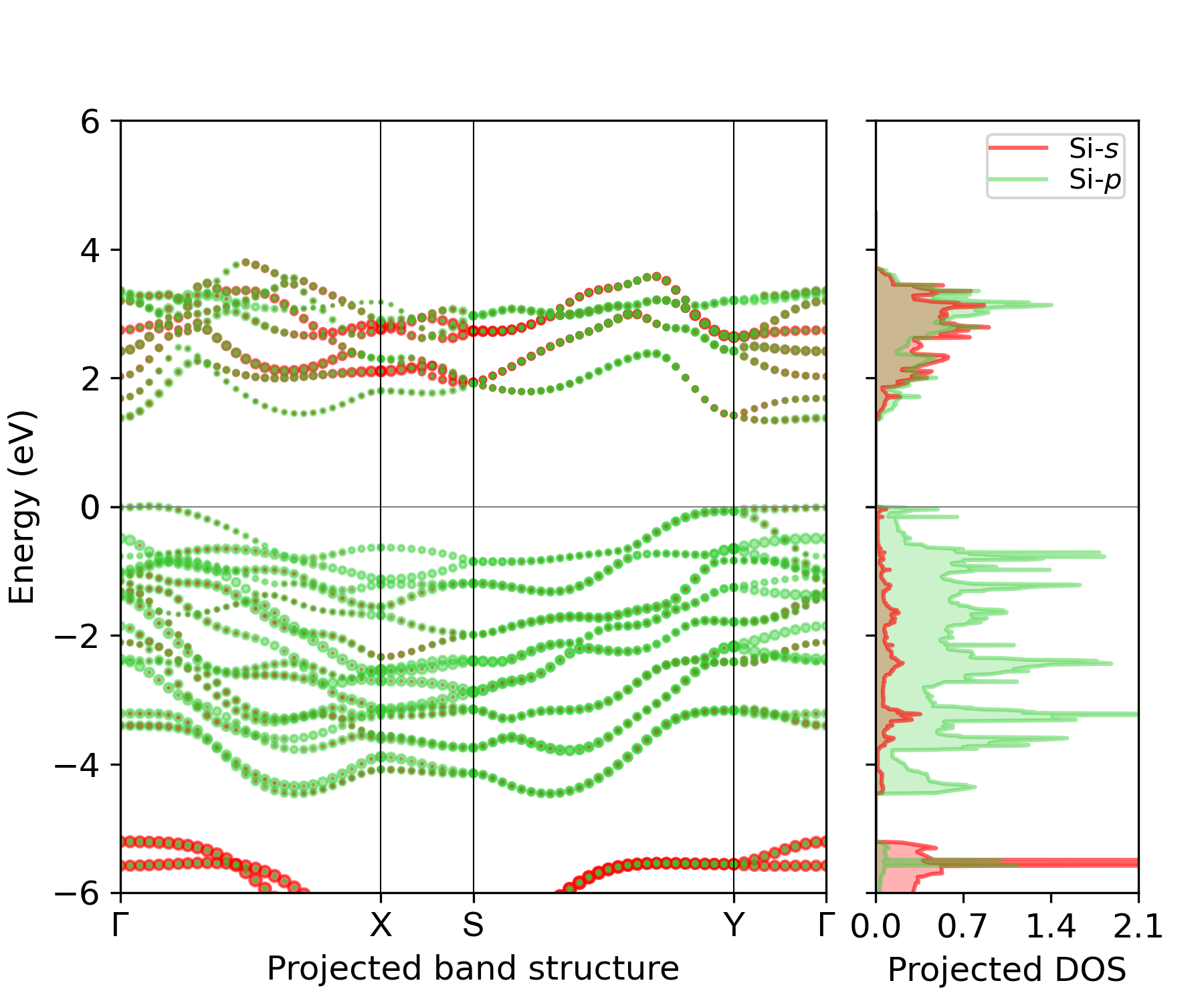
3. Fundmental Electronic Properties
Band Character |
Indirect |
Band Gap (PBE, eV) |
1.3336 |
Band Gap (HSE, eV) |
1.9770 |
Ionization Energy (HSE, eV) |
-5.654 |
Electron Affinity (HSE, eV) |
-3.678 |
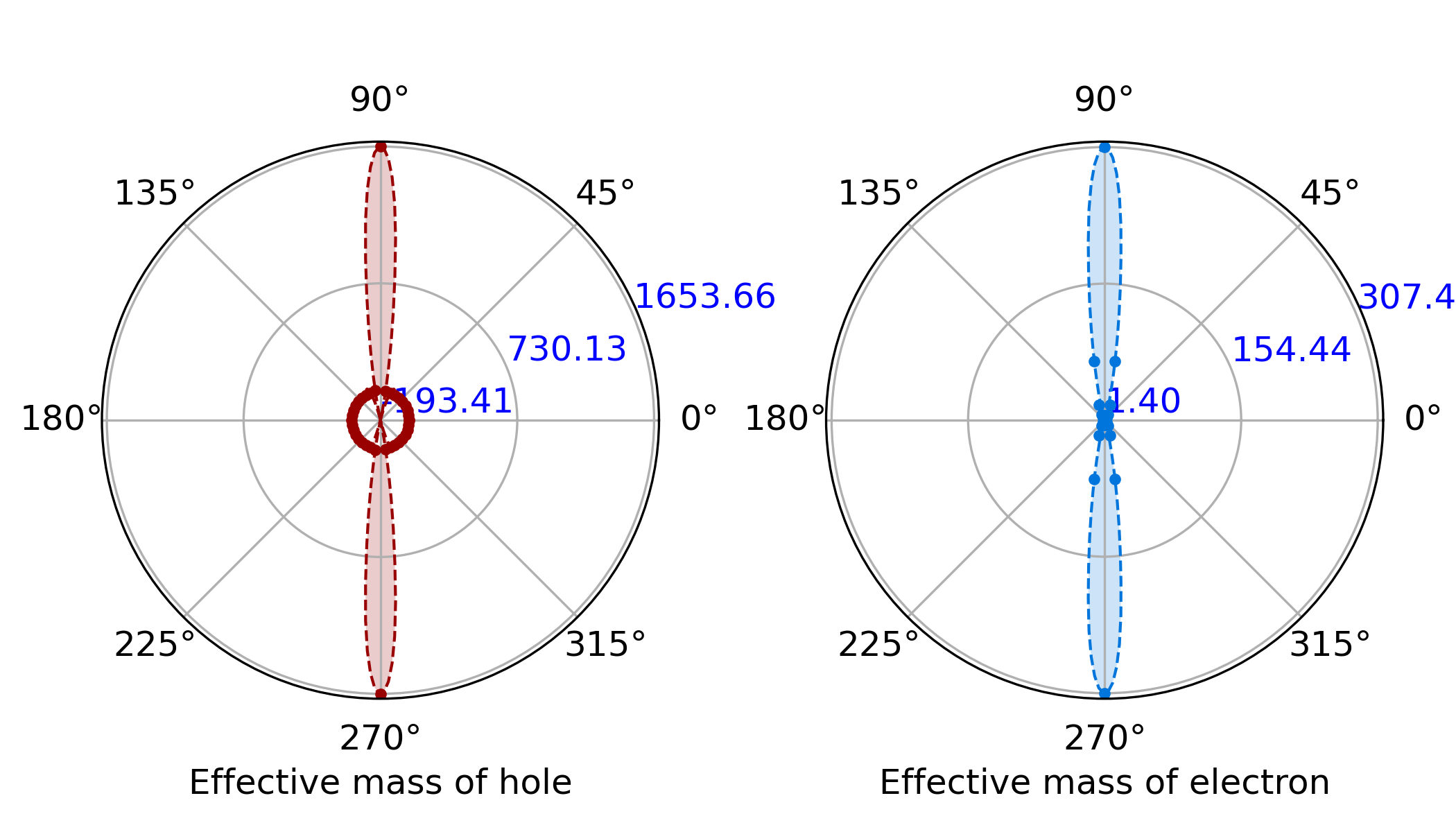
Effective Mass of Electron Max. (m0) |
1653.663 |
Effective Mass of Electron Min. (m0) |
-193.406 |
Effective Mass of Hole Max. (m0) |
307.486 |
Effective Mass of Hole Min. (m0) |
1.402 |
Location of Valence Band Maximum |
[0.058824, 0.058824] |
Location of Conduction Band Minimum |
[0.000000, 0.000000] |
3.1 Global Band Structure (PBE)
3.2 Band Structure and Density of States (PBE)
3.4 Orientation-Dependent effective Masses (PBE)
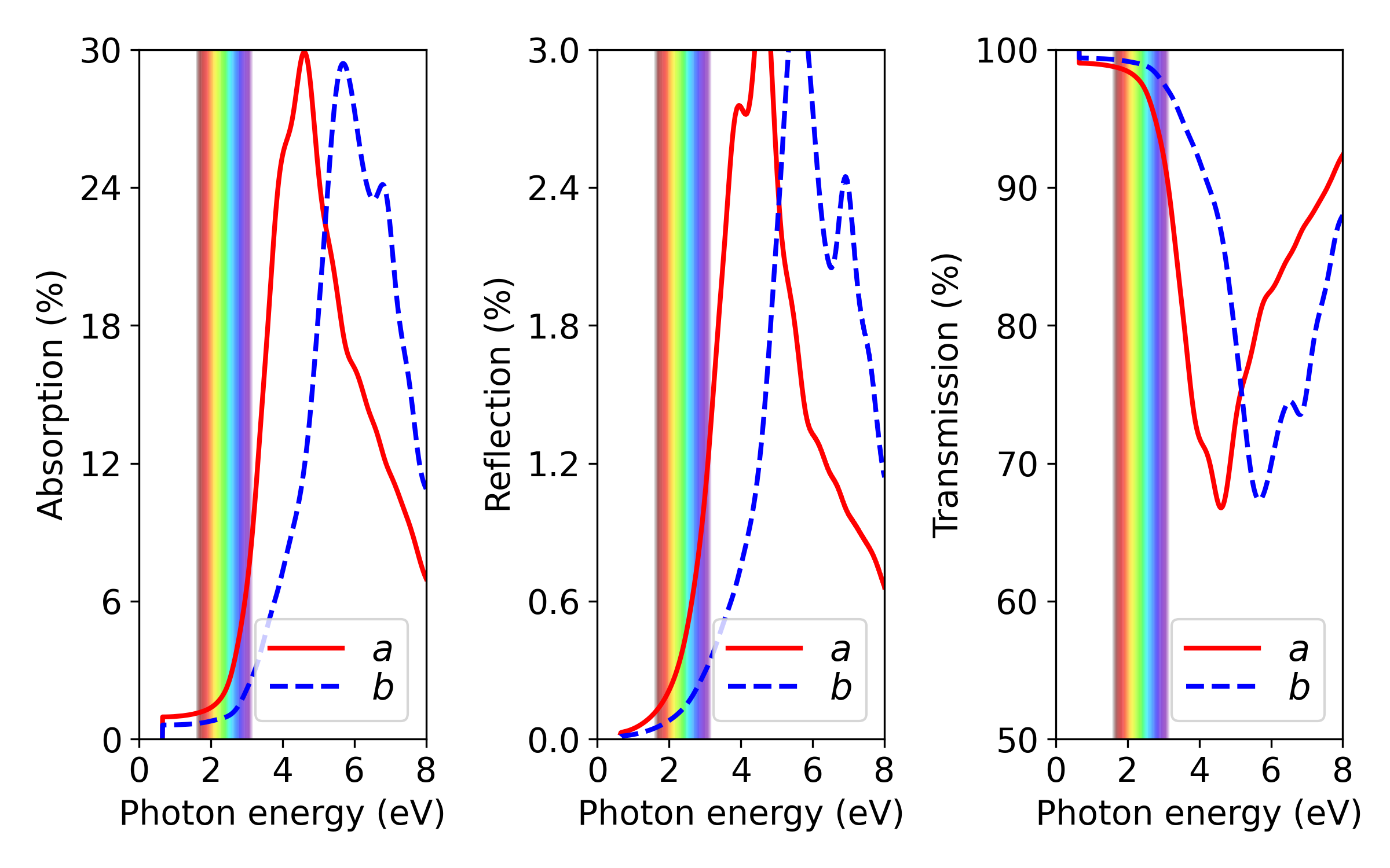
4. Optical Spectrums (HSE)
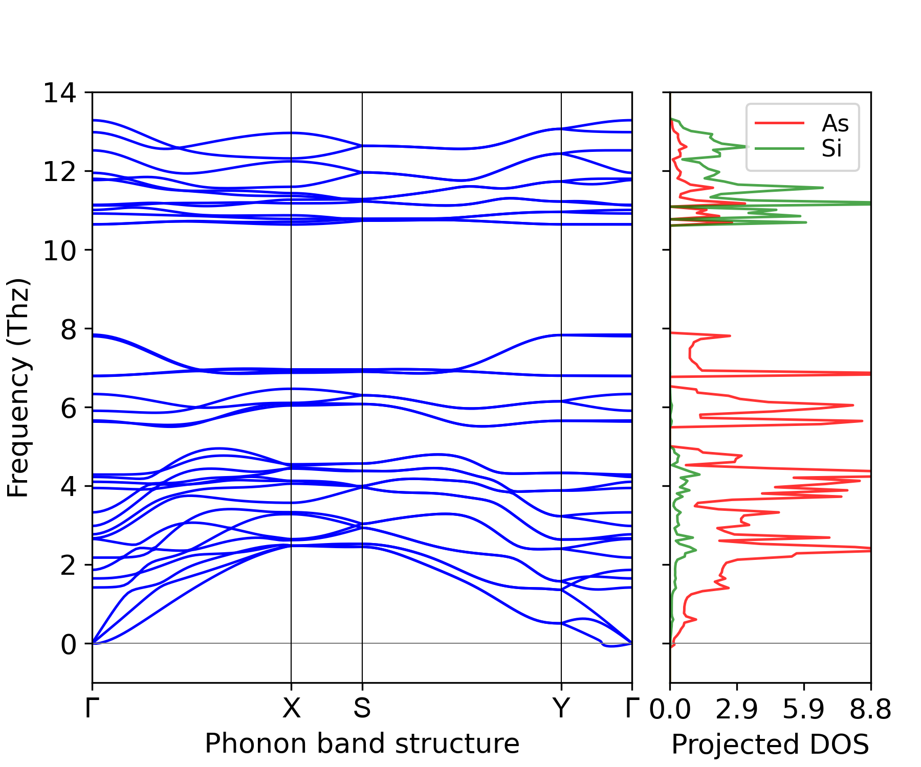
5. Phonon Spectrum and Density of States (PBE)
References
Note
For more details of this database, please refer to the following reference.
[1] V. Wang, G. Tang, Y.-C. Liu, R.-T. Wang, H. Mizuseki, Y. Kawazeo, J. Nara, W.-T. Geng, High-Throughput Computational Screening of Two-Dimensional Semiconductors, Journal of Physical Chemistry Letters 13, 11581 (2022).
License
The contents of this web page are licensed under a Creative Commons 4.0 Attribution International License unless another license is specially mentioned in each web page.